


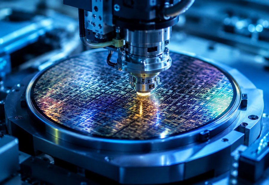
The central government’s “Semicon 2.0” plan could create 150,000 to 200,000 direct and indirect jobs over the next five years. Industry believes this plan will play a key role in transforming India from a mere electronics assembly hub to a global chip design, engineering, and innovation hub .
According to an analysis by NLB Services , a recruitment and workforce solutions company , the next phase of Semicon 2.0 will not be limited to chip manufacturing. It will focus on building a robust ecosystem in areas such as chip design, semiconductor verification, embedded systems, electronic design automation (EDA), AI-based manufacturing, advanced packaging, and smart supply chains.
This assessment comes at a time when the Union Cabinet, chaired by Prime Minister Narendra Modi, recently approved the ₹1.27 lakh crore Semicon 2.0 scheme , which aims to strengthen the design and manufacturing ecosystem in the country.
Sachin Alug, CEO of NLB Services, said that by the year 2030 , the nature of about 70 percent of the jobs in the semiconductor and electronics sector will change , due to which the demand for highly skilled engineers will increase rapidly.
He also said that the number of Global Capability Centers (GCCs) related to the semiconductor sector could increase by 25 to 30 percent by 2030. This will further strengthen India as a global engineering, research and innovation hub.
Experts believe that India’s electronics industry has so far been primarily assembly-based, but through Semicon 2.0, the country will be able to expand its capabilities in high-value areas such as chip design, fabrication, testing and advanced packaging .
Earlier, the India Electronics and Semiconductor Association (IESA) stated that the first phase of the Semicon Mission attracted proposed investments of over $20 billion . The second phase focuses on fabs, advanced packaging, design, research and development, talent development, equipment, and raw materials, enabling India to become a reliable partner in the global supply chain.
According to the government, Semicon 2.0 will focus on six key areas, including chip design, semiconductor equipment and materials, fabrication units, ATMP/OSAT units, research and development, and skill development. So far, the government has approved 12 semiconductor manufacturing projects , with proposed investments of over ₹1.64 lakh crore .
(ADVERTORIAL DISCLAIMER: The above release has been taken from DD News. No editors from The Mainstream were involved in creation of this content.)
Also read: Viksit Workforce for a Viksit Bharat
Do Follow: The Mainstream LinkedIn | The Mainstream Facebook | The Mainstream Youtube | The Mainstream Twitter
About us:
The Mainstream is a premier platform delivering the latest updates and informed perspectives across the technology business and cyber landscape. Built on research-driven, thought leadership and original intellectual property, The Mainstream also curates summits & conferences that convene decision makers to explore how technology reshapes industries and leadership. With a growing presence in India and globally across the Middle East, Africa, ASEAN, the USA, the UK and Australia, The Mainstream carries a vision to bring the latest happenings and insights to 8.2 billion people and to place technology at the centre of conversation for leaders navigating the future.