


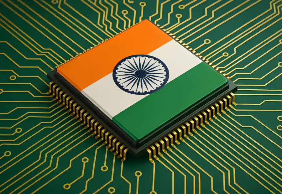
The Union Cabinet, chaired by Prime Minister Narendra Modi, on Wednesday approved Semicon 2.0, a comprehensive programme with a budget outlay of ₹1,27,500 crore aimed at strengthening India’s semiconductor design and manufacturing ecosystem and providing long-term policy support to the sector.
The new programme builds on the momentum generated under Semicon 1.0 and seeks to position India as a major global hub for semiconductor design, manufacturing and innovation through a holistic ecosystem-based approach.
According to the government, Semicon 2.0 has been designed around six key pillars covering chip design, manufacturing equipment and materials, fabrication facilities, semiconductor packaging, research and development, and talent development.
Under the first pillar, the government will strengthen India’s chip design ecosystem. Building on the success of 105 startups that have already begun developing semiconductor chips, the focus will now shift towards creating intellectual property (IP), chip designs and complete systems for both strategic and commercial applications. The initiative aims to establish India as a leading global hub for semiconductor design IP.
The second pillar focuses on promoting the domestic manufacturing of semiconductor equipment, materials, chemicals and specialty gases required for chip production. Companies engaged in manufacturing and research and development of these critical inputs will receive incentives to support the development of a sustainable semiconductor supply chain while also boosting India’s precision manufacturing capabilities.
The third pillar aims to expand semiconductor fabrication capacity by encouraging more global manufacturers to establish fabrication facilities in India. With the country’s first semiconductor fabrication plant expected to be commissioned in 2028, the government plans to attract investments in silicon fabs, compound semiconductor fabs, discrete component fabs and display fabrication units.
The fourth pillar seeks to further strengthen India’s Assembly, Testing, Marking and Packaging (ATMP) and Outsourced Semiconductor Assembly and Test (OSAT) industry. Following the success of existing ATMP projects, the government intends to attract more advanced semiconductor packaging technologies to India and establish the country as an alternative global destination for semiconductor packaging.
The fifth pillar focuses on advancing semiconductor research and development. While India’s semiconductor journey has begun with technologies ranging from 28 nanometres to 110 nanometres, the government now aims to support the development of more advanced semiconductor nodes and next-generation technologies in collaboration with leading research institutions in India and abroad.
The sixth pillar is dedicated to talent development. The government noted that 315 universities across the country are already training students in advanced chip design using industry-standard Electronic Design Automation (EDA) tools, with nearly 68,000 students trained so far. Under Semicon 2.0, this training ecosystem will be expanded further, with greater industry participation in areas such as clean-room operations, semiconductor fabrication, fab construction and related skills.
The government said the programme is expected to support economic growth across multiple sectors, strengthen national security through resilient semiconductor supply chains and enhance India’s technological capabilities in critical industries. By focusing on the entire semiconductor value chain, Semicon 2.0 aims to accelerate both semiconductor design and manufacturing in the country.
Highlighting the progress achieved under India Semiconductor Mission (ISM) 1.0, the government said 12 semiconductor manufacturing projects have so far been approved with a cumulative investment exceeding ₹1.64 lakh crore.
These projects include one silicon fabrication plant, one silicon carbide fabrication unit, an integrated gallium nitride (GaN) Micro LED display fabrication facility and nine semiconductor packaging units. The approved projects are expected to cater to the semiconductor requirements of sectors including consumer electronics, industrial equipment, automobiles, power electronics, telecommunications and aerospace.
Of the 12 approved manufacturing projects, Micron, Kaynes and CG Semi have already commenced commercial production, while another unit is expected to begin production later this year.
On the design front, the government said 24 semiconductor design projects from startups and MSMEs have been approved for financial support. In addition, 105 startups and MSMEs have been provided access to EDA tools.
These companies are developing chips and Systems-on-Chip (SoCs) for a wide range of strategic and commercial applications, including satellite communications, drones, surveillance cameras, Internet of Things (IoT) devices, LED drivers, artificial intelligence systems, telecom equipment and smart meters. The projects are currently at different stages of design and development and are expected to move towards deployment following successful prototyping.
The government said Semicon 2.0 reflects its long-term commitment to establishing India as a global semiconductor powerhouse by strengthening domestic capabilities across design, manufacturing, research, innovation and skilled workforce development.
(ADVERTORIAL DISCLAIMER: The above release has been taken from DD News. No editors from The Mainstream were involved in creation of this content.)
Also read: Viksit Workforce for a Viksit Bharat
Do Follow: The Mainstream LinkedIn | The Mainstream Facebook | The Mainstream Youtube | The Mainstream Twitter
About us:
The Mainstream is a premier platform delivering the latest updates and informed perspectives across the technology business and cyber landscape. Built on research-driven, thought leadership and original intellectual property, The Mainstream also curates summits & conferences that convene decision makers to explore how technology reshapes industries and leadership. With a growing presence in India and globally across the Middle East, Africa, ASEAN, the USA, the UK and Australia, The Mainstream carries a vision to bring the latest happenings and insights to 8.2 billion people and to place technology at the centre of conversation for leaders navigating the future.