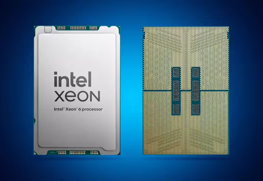
Intel has officially launched its most advanced client and server processors to date — the Intel Core Ultra series 3 (Panther Lake) and Xeon 6+ (Clearwater Forest) — built on its new 18A process node, representing a significant step forward in performance, energy efficiency, and artificial intelligence capabilities.
This launch marks a renewed era of US chipmaking leadership, with both processors being manufactured at Intel’s Fab 52 facility in Chandler, Arizona, part of the company’s $100 billion investment to expand domestic semiconductor production.
Panther Lake, the codename for Core Ultra 3, is aimed at powering next-generation AI PCs, gaming systems, and edge computing devices. It features a scalable, multi-chiplet architecture that gives flexibility across different product segments and price points.
Key highlights of Panther Lake include:
- Up to 16 next-gen P-cores and E-cores delivering over 50% faster CPU performance than the previous generation
- A new Intel® Arc™ GPU with up to 12 Xe cores, offering 50% faster graphics performance
- A balanced XPU architecture delivering up to 180 TOPS for AI acceleration
- Intel is also expanding Panther Lake’s reach into edge applications such as robotics, supported by its new Intel Robotics AI software suite and a dedicated reference board to enable real-time robot control and perception.
- The Xeon 6+ processor, codenamed Clearwater Forest, is Intel’s first server chip built on the 18A process. It is designed for hyperscale data centres, cloud providers, and telecom networks, and is expected to launch in the first half of 2026.
Xeon 6+ will offer:
- Up to 288 efficient cores (E-cores)
- A 17% increase in Instructions Per Cycle (IPC) over the previous generation
- Both Panther Lake and Xeon 6+ are built on Intel 18A, the first 2-nanometre-class node developed and manufactured in the US. The process offers 15% better performance per watt and 30% higher chip density compared to Intel 3.
Core innovations include:
- RibbonFET, Intel’s new transistor architecture for better scaling
- PowerVia, a backside power delivery system for improved energy flow
- Foveros 3D stacking, allowing integration of multiple chiplets into advanced system-on-chip designs
Intel CEO Lip-Bu Tan said, “We are entering an exciting new era of computing, made possible by great leaps forward in semiconductor technology that will shape the future for decades to come.”
Tan added, “The United States has always been home to Intel’s most advanced R&D, product design and manufacturing – and we are proud to build on this legacy as we expand our domestic operations and bring new innovations to the market.”
Intel’s innovations and local manufacturing efforts reinforce its role in building a resilient and self-reliant semiconductor supply chain, benefitting both its internal product lines and global foundry customers.
Also read: Viksit Workforce for a Viksit Bharat
Do Follow: The Mainstream formerly known as CIO News LinkedIn Account | The Mainstream formerly known as CIO News Facebook | The Mainstream formerly known as CIO News Youtube | The Mainstream formerly known as CIO News Twitter |The Mainstream formerly known as CIO News Whatsapp Channel | The Mainstream formerly known as CIO News Instagram
About us:
The Mainstream formerly known as CIO News is a premier platform dedicated to delivering latest news, updates, and insights from the tech industry. With its strong foundation of intellectual property and thought leadership, the platform is well-positioned to stay ahead of the curve and lead conversations about how technology shapes our world. From its early days as CIO News to its rebranding as The Mainstream on November 28, 2024, it has been expanding its global reach, targeting key markets in the Middle East & Africa, ASEAN, the USA, and the UK. The Mainstream is a vision to put technology at the center of every conversation, inspiring professionals and organizations to embrace the future of tech.


