


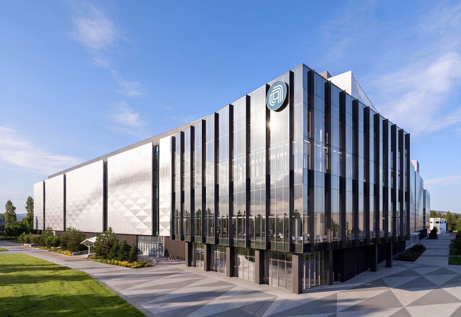
Applied Materials has opened a major research facility in Sunnyvale, California, designed to bring chipmakers, equipment suppliers and university researchers together to accelerate the development of next-generation semiconductor technologies.
The new facility, called the Equipment and Process Innovation and Commercialization (EPIC) Center, represents a planned investment of approximately $5 billion. It aims to help the semiconductor industry move innovations from research laboratories to large-scale manufacturing more quickly.
The center brings together some of the world’s leading semiconductor companies, including TSMC, Intel, Samsung Electronics, Micron Technology and SK hynix as founding partners. Other innovation partners include Broadcom, Advantest, SCREEN, Kioxia and Besi.
Researchers from universities such as Stanford, UC Berkeley, UCLA, Arizona State University and Rensselaer Polytechnic Institute will also collaborate with Applied Materials’ scientists and engineers at the facility.
Collaboration to address AI chip challenges
The investment comes as developing advanced AI chips becomes increasingly complex and expensive. Modern AI systems require improvements not only in processors but also in memory, data-transfer connections and advanced packaging technologies that integrate different components.
Progress in one area often depends on advances in others, making collaboration across the semiconductor ecosystem increasingly important.
Applied Materials, a supplier of semiconductor manufacturing equipment, aims to address this challenge through a coordinated research model. Instead of developing materials, equipment and manufacturing processes in separate stages, the EPIC Center will allow teams to work on these technologies simultaneously.
Engineers from chipmakers and equipment suppliers will work alongside researchers developing the underlying technologies. According to Applied Materials, this approach is expected to shorten development cycles and help manufacturers introduce new processes into high-volume production sooner.
However, these benefits remain goals of the project and have not yet been publicly demonstrated.
A large-scale research and manufacturing facility
The EPIC Center covers approximately 600,000 square feet and includes nearly 4 acres of advanced cleanroom space. Applied Materials said construction required more than 6 million labour hours.
The company expects its capital spending on the facility to increase gradually towards approximately $5 billion as customer projects begin. This means the full amount represents a planned investment over time rather than money already spent.
Through the EPIC Center, Applied Materials aims to improve collaboration across the semiconductor industry and accelerate the development of manufacturing technologies needed for future generations of AI chips.
Also read: Viksit Workforce for a Viksit Bharat
Do Follow: The Mainstream LinkedIn | The Mainstream Facebook | The Mainstream Youtube | The Mainstream Twitter
About us:
The Mainstream is a premier platform delivering the latest updates and informed perspectives across the technology business and cyber landscape. Built on research-driven, thought leadership and original intellectual property, The Mainstream also curates summits & conferences that convene decision makers to explore how technology reshapes industries and leadership. With a growing presence in India and globally across the Middle East, Africa, ASEAN, the USA, the UK and Australia, The Mainstream carries a vision to bring the latest happenings and insights to 8.2 billion people and to place technology at the centre of conversation for leaders navigating the future.