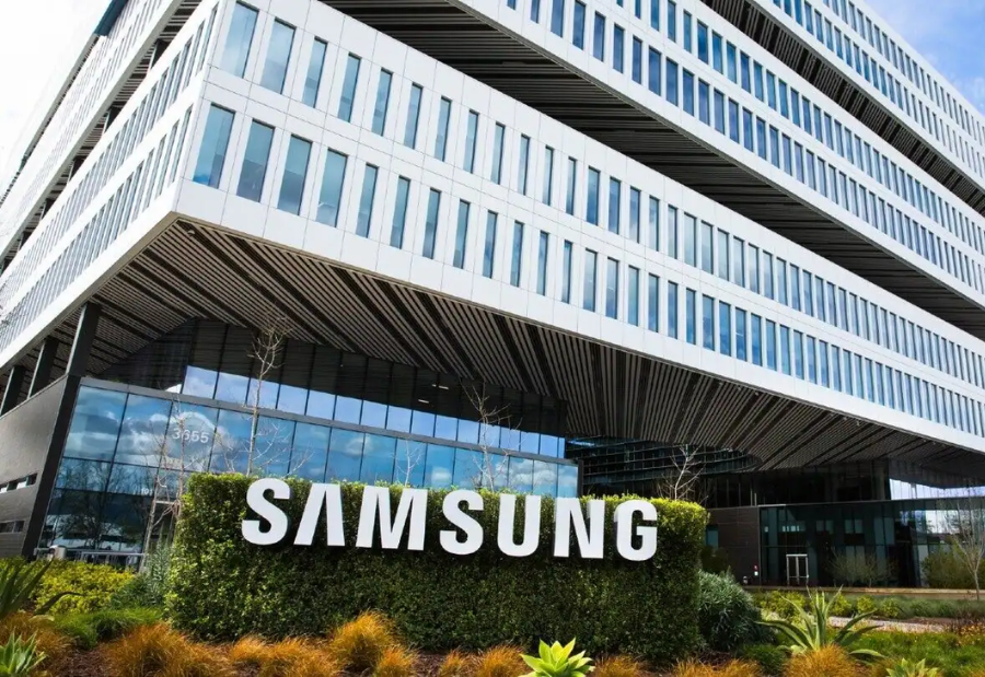
South Korean technology giant Samsung Electronics is intensifying its efforts to attract semiconductor talent in India, recognising the country as a growing centre for chip design and innovation, according to a report by a common news source.
On Monday, Samsung Semiconductor India Research (SSIR) announced multiple openings for research and development engineers across its key semiconductor divisions, including System LSI, memory, and foundry. The move is part of Samsung’s broader global strategy to enhance its semiconductor design leadership and competitiveness in artificial intelligence (AI) and high-performance computing (HPC).
According to the report, SSIR is hiring for 16 specialised positions such as system-on-chip (SoC) design engineers, memory design engineers, SSD firmware engineers, and graphics driver developers. These roles are central to the development of next-generation technologies, including system semiconductor integration, memory architecture, firmware optimisation, and AI computation efficiency.
Sources familiar with the matter said that Samsung aims to evolve SSIR from a research support unit into one of its global design hubs for AI-driven semiconductors.
In a move to strengthen local leadership, Samsung recently appointed Rajesh Krishnan, an experienced professional in the memory sector, as the new head of SSIR. His appointment reflects the company’s shift towards a talent-driven research and development model led by local expertise.
Based in Bengaluru, SSIR is a key component of Samsung’s global semiconductor ecosystem and plays a vital role in advancing the three major pillars of its Device Solutions division: memory, System LSI, and foundry technologies.
Samsung’s growing focus on nurturing Indian talent also aligns with the government’s Semicon India initiative, which aims to build a robust domestic semiconductor ecosystem. The Indian semiconductor market is projected to reach USD 100 billion by 2030, attracting significant investments from global players such as Micron Technology.
“Samsung’s latest actions appear to be a strategic move to position India as one of its core global semiconductor design hubs in the AI era,” an industry official was quoted as saying.
Also read: Viksit Workforce for a Viksit Bharat
Do Follow: The Mainstream formerly known as CIO News LinkedIn Account | The Mainstream formerly known as CIO News Facebook | The Mainstream formerly known as CIO News Youtube | The Mainstream formerly known as CIO News Twitter |The Mainstream formerly known as CIO News Whatsapp Channel | The Mainstream formerly known as CIO News Instagram
About us:
The Mainstream formerly known as CIO News is a premier platform dedicated to delivering latest news, updates, and insights from the tech industry. With its strong foundation of intellectual property and thought leadership, the platform is well-positioned to stay ahead of the curve and lead conversations about how technology shapes our world. From its early days as CIO News to its rebranding as The Mainstream on November 28, 2024, it has been expanding its global reach, targeting key markets in the Middle East & Africa, ASEAN, the USA, and the UK. The Mainstream is a vision to put technology at the center of every conversation, inspiring professionals and organizations to embrace the future of tech.


