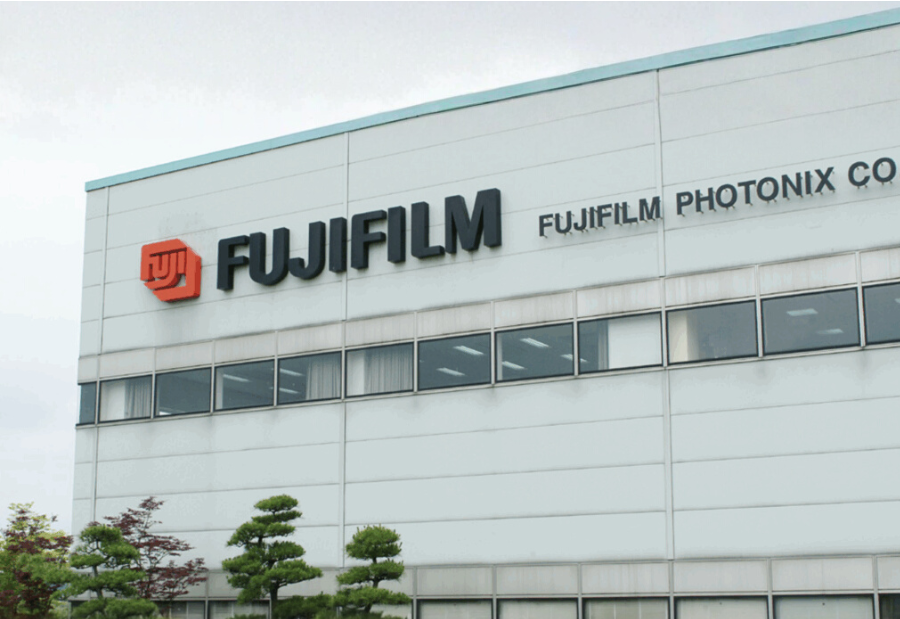
Fujifilm Corporation in Japan has opened a new development and evaluation building at its Shizuoka Factory. The facility began operations this month and marks a major step in strengthening the company’s semiconductor materials business.
The investment increases Fujifilm’s ability to evaluate performance and quality. It will help speed up the development of advanced and next generation semiconductor materials while supporting a stable supply of high quality products. The move comes at a time when global demand for semiconductors used in artificial intelligence, fifth generation networks, and the internet of things continues to grow.
Fujifilm’s semiconductor materials business has seen sales almost double between the financial years of 2021 and 2024. It has now become a major growth driver for the group. To support this expansion, the company invested more than one hundred billion yen in its facilities from the financial years of 2021 to 2024. It plans to invest more than one hundred billion yen again from the financial years of 2025 to 2026.
The new building at Shizuoka includes cleanrooms with high cleanliness standards, modern evaluation equipment, and inspection systems powered by artificial intelligence. These systems detect very small particles to improve analysis accuracy and quality control.
A dedicated digital transformation department will also use artificial intelligence and digital tools to improve manufacturing processes. The building uses an RC column head seismic isolation structure for safety. Its cleanroom is placed twelve metres above ground level to reduce the risk of flooding.
The Shizuoka Factory works with Fujifilm’s global research and development and production sites. It supports next generation process technologies around the world. With this new facility, Fujifilm aims to speed up the development of advanced EUV, ArF, NIL, PFAS free materials, and its Wave Control Mosiac technology. This reinforces its position in the future of semiconductor innovation.
Also read: Viksit Workforce for a Viksit Bharat
Do Follow: The Mainstream formerly known as CIO News LinkedIn Account | The Mainstream formerly known as CIO News Facebook | The Mainstream formerly known as CIO News Youtube | The Mainstream formerly known as CIO News Twitter
About us:
The Mainstream is a premier platform delivering the latest updates and informed perspectives across the technology business and cyber landscape. Built on research-driven, thought leadership and original intellectual property, The Mainstream also curates summits & conferences that convene decision makers to explore how technology reshapes industries and leadership. With a growing presence in India and globally across the Middle East, Africa, ASEAN, the USA, the UK and Australia, The Mainstream carries a vision to bring the latest happenings and insights to 8.2 billion people and to place technology at the centre of conversation for leaders navigating the future.


